Scanning tunneling microscopy & spectroscopy
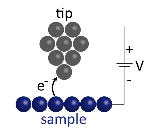 There are many experimental techniques that probe different aspects of exotic properties of materials, such as superconductivity or colossal magnetoresistance, to get a better understanding of the microscopic origin of these properties. The strength of a scanning tunneling microscope (STM) is that it can address the important players (the electrons, the lattice and the spins) at the scale where the action takes place: the atomic scale. The STM essentially is no more than a sharp needle, or tip, that is brought in close proximity to (but without touching) the surface of a material. A non-zero current will be established from one to the other upon applying a voltage difference between the sample and the tip when these are close enough. To a good approximation, the tip-sample distance (d) dependence of the current (I) is given by:
.png) where κ is a material dependent constant that for typical metals such as gold and copper is on the order of 1 Å-1. Changing the distance by 1 Å, i.e. 0.1 nm, therefore changes the current by a factor e=2.72. This extreme height sensitivity is used to image the atomic lattice with high precision. If the density of states, g(r,E), is position independent, the exact height profile of the surface can be mapped by monitoring the change in tip height to keep the current constant while scanning across the surface. On the left is an example of such a constant current image, showing clearly the atomic lattice of in this case the iron based superconductor Fe(Se,Te). Usually, however, the density of states is not constant as function of position - this is what makes the materials so interesting - and a convolution of height and g(r,E) is obtained. Without going into the derivation (see e.g. 1), at sufficiently low temperatures the elastic tunneling current from sample to tip for a voltage V applied to the sample can be described by:
where κ is a material dependent constant that for typical metals such as gold and copper is on the order of 1 Å-1. Changing the distance by 1 Å, i.e. 0.1 nm, therefore changes the current by a factor e=2.72. This extreme height sensitivity is used to image the atomic lattice with high precision. If the density of states, g(r,E), is position independent, the exact height profile of the surface can be mapped by monitoring the change in tip height to keep the current constant while scanning across the surface. On the left is an example of such a constant current image, showing clearly the atomic lattice of in this case the iron based superconductor Fe(Se,Te). Usually, however, the density of states is not constant as function of position - this is what makes the materials so interesting - and a convolution of height and g(r,E) is obtained. Without going into the derivation (see e.g. 1), at sufficiently low temperatures the elastic tunneling current from sample to tip for a voltage V applied to the sample can be described by:
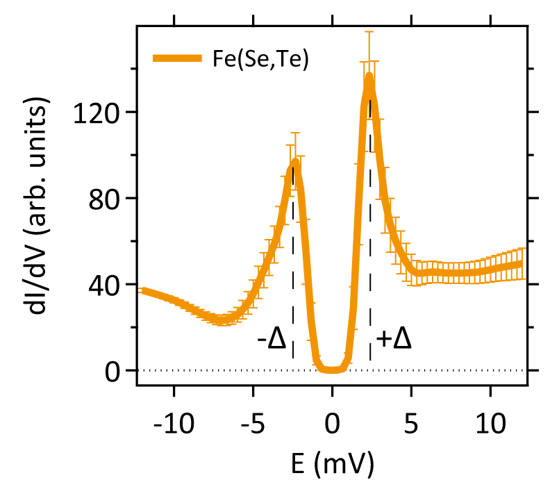 where gtip(0) is the energy independent density of states of the tip, e is the elemental charge, f is the Fermi-Dirac distribution function and M are matrix tunneling elements. Usually, |M|2 is sufficiently energy independent to take it in out of the integral: the current is then directly proportional to the integral of the density of states of the sample. Its derivative, the differential conductance, dI/dV, is then directly proportional to the density of states. A measurement of the differential conductance as a function of bias voltage is thus directly proportional to the energy dependence of the density of states. The plot on the right shows a typical dI/dV spectrum of a superconductor, with prominent superconducting coherence peaks at ± Δ.
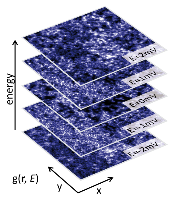 More importantly, the measurements of the density of states can be done on the atomic scale. By combining the constant current imaging mode with energy dependent spectroscopy, a three dimensional dataset of the energy and atomic scale position of the density of states can be recorded. These 3D blocks of data contain all the ingredients to extract for instance the superconducting gap structure, the vortex lattice, the band structure, etc.
In some cases |M|2 does have a pronounced energy dependence, leading to a dependence of the results on the junction resistance (also called the 'setup effect'). Normalisation of the differential conductance by the conductance, (dI/dV)/(I), is in many cases a good method to remove the systematic error introduced by the matrix tunnel elements 2.
The energy resolution of the STM is determined by the measurement temperature. Since tunneling involves electrons jumping from the tip to the sample or vice versa, smearing due to finite temperature is given by the full width half maximum (FWHM) of the product of their respective Fermi-Dirac distributions:
and thus
.
This result is the theoretical limit of the energy resolution and can for various reasons be slightly worse. Typical measurements at 4.2 K have therefore an energy resolution of roughly 1.25 mV.
1. J. Chen, Introduction to scanning tunneling microscopy, Oxford University Press, 1993↩
2. R. M. Feenstra, Surface Science 181, 295 (1987)↩